
26.11.2015
SMT production plant as the final touch on the way to lean factory
FEIG ELECTRONIC lays the foundation for further growth
„Fit for the Future“ describes a LEAN project at FEIG ELECTRONIC, which defines the implementation of a continuous improvement process (CIP) as a target. For this, enterprise- wide overages were identified and waste-free, cost-optimized processes and standards have been implemented. An example of optimized processes is the new SMT production plant, which started production on 11/20/2015.
Increase of value added and vertical integration through insourcing
Within the production department the most extensive projects were carried out.
By implementing process-optimizing measures such as the transition to island production efficiency, significant improvements have been achieved while reducing production time per item.
First, a new manufacturing area called "Manual Assembly (THT) and Selective Soldering" was established. This helped to increase the level of vertical integration and value creation. With start-up of the new SMT production process on November 20-2015, automatic assembly of printed circuit boards on the pinnacle of manufacturing technology at FEIG ELECTRONIC was introduced. Currently, all production processes are combined under one roof.
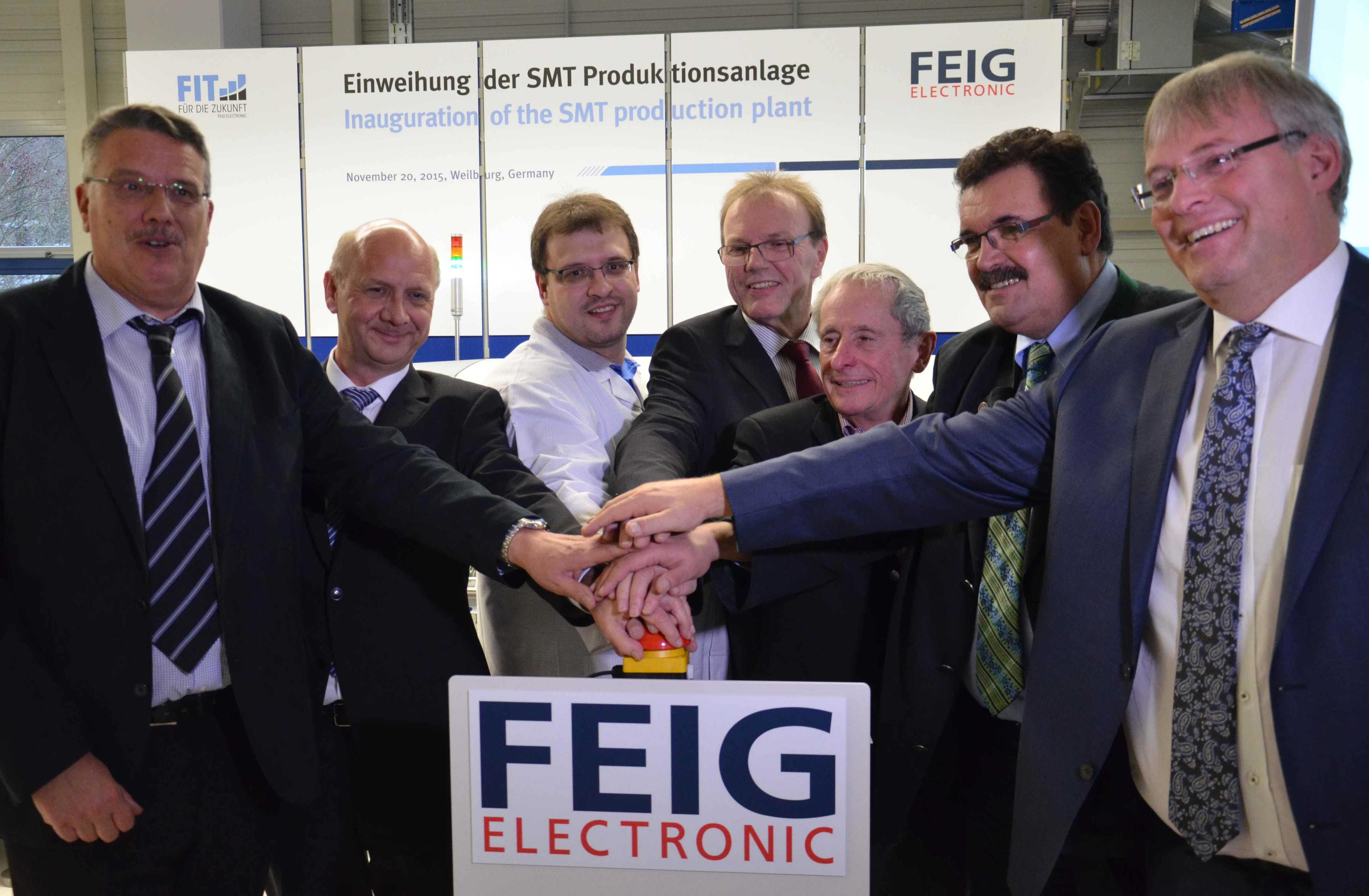
On 11/20/2015 all employees of FEIG ELECTRONIC, and numerous honorary guests, gathered on the production floor. After a welcoming speech by company founder and owner, Mr. Wolfgang Feig, the General Manager of FEIG ELECTRONIC GmbH, Mr. Eldor Walk, presented the company's evolution since its foundation in 1966. The company’s fields of activity, employee structure, and development prospects for the future were outlined. Following introduction of several guest politicians and business owners, who greeted the audience, Production manager, Mr. Rudolf Dörr, spoke to the audience. Mr. Dörr briefly outlined changes in production as part of this LEAN project, culminating in expanding vertical integration. Realized value was added by integrating the new SMT assembler to the automatic PCB production line.
A group of seven individuals initialized production by de-pressing the system actuator.
Following initialization, Mr. Tobias Fickus, the head of the SMT production, explained the process the PCB encounters to become a finished assembled component. For this special event and it’s proximity to Christmas, neither a PCB for a door controller nor for a RFID reader was produced. But instead, a small Christmas tree PCB was produced. This PCB tree was equipped with seven red LEDs, a battery receptacle, and a USB port. The USB port can be used to power the tree without battery. Each participant of the ceremony was gifted with a PCB tree.
All processes under one roof ensure maximum flexibility
With the introduction of SMT technology FEIG ELECTRONIC offers a wider range of manufacturing capabilities, which provides maximum flexibility in terms of meeting customer requirements.
Reliance upon external partners has been drastically reduced. Close integration of the development department with product manufacturing ensures optimum production processes and increases on-time deliveries.
During a typical 8-hour shift production is currently integrating 127,000 components
The statistical data regarding the new SMT production line is impressive. Plans are being drawn to expand to a second SMT line in 2016, resulting in a total investment of approximately 2.5 million euros . This two-line system will have the capacity to assemble 80 million components per year utilizing a mix of processors, resistors, and capacitors.
FEIG ELECTRONIC currently integrate 1,600 different components within the SMT production line, producing 270 different types of PCB’s.
Approximately 400,000 assembled PCB’s are produced each year, comprising various FEIG products utilized in door controllers, loop detectors, RFID readers, and payment systems.
Various production steps may require higher forms of training
In order to complete a PCB, six different production steps must be performed.
First, the production area must be configured to produce a specific product. Depending on the complexity of the module, a preparation and tooling time of 0.5 to 6 hours is required. The second step is the application of the solder paste to the PCB. The third step is the actual PCB assembly. The fourth step is the so-called "reflow soldering". Here, the components are exposed to a furnace at high temperature, enabling the components to fuse together. Step Five is an automatic optical inspection. The final step is inspection of all rejected units. If required, manual rework will de done. These production steps are performed in 2 shifts of 8 hours. Production for this area of assembly is performed by employees with requiring specialized training.
Securing existing jobs and creating new jobs through steady growth
FEIG ELECTRONIC currently has approximately 250 employees, making it one of the largest employers in the region. This owner-managed, medium-sized, high-tech company operates within four product areas; CONTROLLER, SENSORS, RFID, and PAYMENT. FEIG ELECTRONIC is a technology leader known worldwide in various markets.
The company invests in the ongoing expansion of its product areas by adding new products for increasingly innovative applications, as well as entry into new market segments. Due to our continued growth, twenty new positions will become available for all divisions in 2016, specifically targeting development departments.
Employment at FEIG ELECTRONIC is highly sought after. In addition to a modern work environment, and advanced technological equipment, the company offers a desirable work- life balance. Flexible working hours, overtime compensation, its own canteen, and a FEIG- child-care facility. These benefits are not typical for a company of this size. A culture of open communication between employees and supervisors, as well as granting the greatest possible creative freedom in achieving objectives, provides a family style atmosphere.